Prof. Radimír Vrba (head)
Prof. Lubomír Grmela (vice-head)
Vision and mission:
Research in the programme of Sensor Systems is focused on the investigation of advanced sensor systems, analysis of appropriate diagnostic methods for complex testing of such systems, and the design of ordered nanostructures of various shapes on nanosensor electrodes. Attention is turned to the investigation of the magnitude and sensitivity of signals, including their transmission and evaluation. The research programme likewise includes the development of new methods for the diagnostics and characterization of materials and electrical components, which is necessary to meet new requirements for the sensing of both electrical and non-electrical quantities.
Areas of expertise:
Characterization of materials and structures
We have long-term experience with various characterizations of materials and structures in wide ranges of frequencies and temperatures (from 10 K). We provide dielectric characterization of materials (solids/liquids), characterization of passive components, and characterization of semiconducting material and components in temperature range 10 K – 400 K by using wide spectrum of laboratory equipment. We are able to identify structural parameters, such as charge carriers concentration, mean lifetime, PN junction type, etc. We provide local optical and electronic characterization of optoelectronic structures with lateral resolution better than 100 nm. We evaluate a structure quality (local and bulk defects, contacts) and provide an investigation of structural parameters both under standard conditions and under extreme thermal conditions. We have developed several new methods with corresponding instruments for material characterizations (e.g. the device for measurement of the distribution of surface potential on a material structure).
Performing of loading test and diagnostics of materials under tests
We provide artificial aging by using long-term thermal cyclic loading with/without guaranteed level of relative humidity as well as provide accelerated aging by using the method of current pulses. We are able to identify an origin of microcracks inside nonconductive materials and electrical components by using electromagnetic and acoustic emission.
Optimization of structures
Based on our capabilities of material characterizations, we have extensive experience in development of physical models of components/sensors to optimize their parameters. We also provide optimization of signal-to-noise ratio of sensors on the basis of electrical and noise characteristics.
Measurements of noise and transport characteristics
Using the state-of-the art equipment, we provide measurements of the time dependences of noise voltage and noise currents, measurements of noise spectral densities, measurements of voltage and current dependences of the RMS value of narrowband noise current, and transport characteristics measurements (VA characteristics with voltage source or current source, CU characteristics up to 600 V).
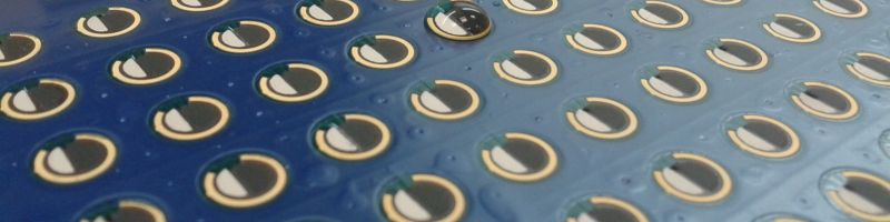
Electrochemical sensors and biosensors
We have extensive experience in development of electrochemical methods for species determination. We are able to design the electrodes as paste and printed on several substrates, their modification towards high sensitivity including nanoparticles incorporation on the surface of electrodes. Biosensing methods suitable for pharmacy and medicine are also topic of our know-how.
Nanostructured devices
Our research expertise in nanostructured devices deals with preparation of highly ordered nanostructured surfaces with ordered nanodots, nanocolumns, and nanowires preparation using non-lithographic methods. The technologies enable to create nanosensors, hydrophobic surfaces, porous structures for high surface planar devices, fluorescent surfaces, nanoelectrodes and 3D nanostructures.
Full custom integrated circuit design
The ASIC research team is composed of scientists, who have wide theoretical and practical knowledge about ICs, AD and DA converters, microelectronics, microprocessor architecture design, HW/SW co-design, low-power rtl synthesis (RTL Compiler) , mixed-mode IC design, small signal processing, Opamp offset compensation, digital filter design, low-power physical implementation (SOC Encounter), ASIC design for smart sensor signal processing, communication interface design (SPI, I2C etc.) and computer aided simulation of electronic circuits.
Geolocation
Our research expertise in Geolocation deals with location of nodes in IP and sensor networks. We are able to locate the nodes using the current state of the art measurement-based methods. We have experience with the research network PlanetLab with over 1000 IP nodes spread over the whole world. For the location in sensor network, we own a large-scale wireless network based on the 6LoWPAN standard.